Intel Unveils Detailed Roadmap for 14A Node and Beyond at J.P. Morgan TMT Conference
At the recent J.P. Morgan TMT Conference, Intel CEO Lip-Bu Tan shared significant updates on Intel’s advanced semiconductor manufacturing roadmap. The company is now targeting a risk production run for its 14A process node in 2028, with high-volume manufacturing (HVM) expected to commence in 2029. This timeline aligns closely with the anticipated launch of TSMC’s A14 node, setting the stage for direct competition in the next generation of angstrom-class semiconductor technology.
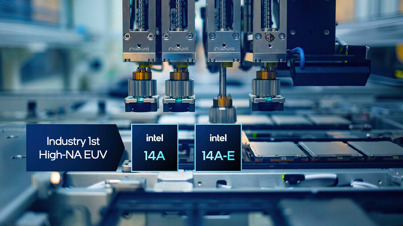
14A Node: Accelerated Progress and Advanced Lithography
Intel’s 14A node is progressing at a notably faster and more efficient pace compared to the earlier 18A node. Early development has shown improved yields and a less complex manufacturing process, signaling a smoother path to mass production. A key innovation with 14A is its adoption of ASML’s High-NA EUV (Extreme Ultraviolet) lithography tools, marking the first time this cutting-edge technology will be used in global semiconductor manufacturing. High-NA EUV represents a significant leap in chip fabrication, enabling finer features and greater transistor density.
Currently, the 14A node is at the 0.5 Process Design Kit (PDK) stage. Intel plans to release the 0.9 PDK—described by Lip-Bu Tan as the “holy grail” for customers—in October. This milestone will allow customers to finalize their designs and requirements, paving the way for the next phase of development and eventual high-volume production.
Expanding the Roadmap: 10A and 7A Nodes on the Horizon
Looking beyond 14A, Intel is already planning for future nodes, specifically the 10A and 7A process technologies. These additions to the roadmap reflect Intel’s commitment to continuous innovation and long-term technology evolution, both for its own products and for third-party foundry customers. By providing a clear and forward-looking roadmap, Intel aims to offer the predictability and investment confidence that major customers seek when choosing a semiconductor foundry partner.
This strategic approach mirrors the model established by TSMC, where customers are encouraged to engage early and plan for future nodes. Intel’s goal is to become a trusted foundry partner with a robust, long-term roadmap, supporting the needs of both internal product teams and external clients as the semiconductor industry enters the angstrom era.